
Today's digital cameras are basically based on charge coupled device (CCD) or CMOS sensor technology. Both of these technologies can convert optical signals into electrical signals, but their conversion methods are different.
Today's digital cameras are basically based on charge coupled device (CCD) or CMOS sensor technology. Both of these technologies can convert optical signals into electrical signals, but their conversion methods are different.
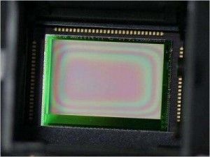
In the CCD component, an array of millions of photosensitive pixels covers the surface of the CCD sensor. After the sensor is exposed, first the end of the CCD reads out the accumulated charge covering the entire CCD pixel array, and then is digitized by the analog front end (AFE) chip or CCD processor. Another kind of sensor, CMOS sensor can directly digitize the exposure level of each pixel unit.
Generally, CCD has the highest image quality and lowest noise, but its power consumption is higher. CMOS sensors are easy to manufacture and have low power consumption characteristics, but their image quality is low. Part of the reason is because the transistor located in each pixel easily blocks part of the light signal reaching the pixel. However, if the price is compared with CCD in the process of quality competition, then CMOS has an advantage, and the number of mid-range digital cameras using CMOS sensors is increasing.
Regardless of the type of sensor used in the digital camera, all pixels of the sensor array need to be sensitive to gray levels-from fully dark (black) to fully bright (white). The sensitivity to gray levels is called "bit depth". Therefore, 8 bit pixels can distinguish 28 or 256 gray gradients, while 12 bit pixels can distinguish 4096 gray gradients. The layered entire pixel array is a color filter that divides each pixel into several color-sensitive "sub-pixels". This arrangement allows the measurement of the different color components of each pixel unit. Therefore, the color of each pixel unit can be regarded as the sum of red (R), green (G) and blue (B) channel light components superimposed in an additive manner. The higher the bit depth, the richer the colors that RGB space can produce. For example, 24-bit color (8 bits per channel for R, G, and B) can produce 224 or 16.7 million discrete colors.
In order to properly represent a color image, each pixel unit, each sensor requires 3 color samples-most commonly R, G, and B. However, having 3 separate sensors for each digital camera is not a cost-effective solution (although this solution has become more practical recently). Moreover, when the resolution of the sensor increases to 5-10 million pixels, some image compression formats will be required to prevent the need to output 3 bytes for each pixel unit (or worse, for higher resolution Sensor, it will also need to output 3 12-bit words).
Don't worry, because digital camera manufacturers have developed clever ways to reduce the number of necessary color samples. The most common method is to use a color filter array (CFA), which only measures one color of any given pixel unit. Then, use the image processor to interpolate the measurement results so that it looks as if 3 colors are measured in each pixel unit.
The most popular CFA used today is the Bayer model, as shown in Figure 1. The scheme was founded by Kodak, which uses the principle that the human eye is more sensitive to green components than red or blue. Therefore, in the Bayer filter array, the intensity of light passing through the green filter is twice that of the blue filter or the red filter. This leads to an output format commonly referred to as "4:2:2 RGB", that is, every time 2 red light and 2 blue light are sent, 4 green light is sent.

Bayer mode image sensor arrangement
Image sensor connection
CMOS sensors usually output the parallel data stream of the pixel unit in YCbCr or RGB format, accompanied by horizontal and vertical synchronization and pixel clock. Sometimes they allow the use of external clocks and synchronization signals to control the frame image output from the sensor.
On the other hand, CCD sensors usually need to be connected to an "analog front end (AFE)" chip, such as AD9948, which can process the analog output signal, digitize it, and generate the appropriate timing for scanning the CCD array. The processor provides the synchronization signal for the AFE, and it needs this control signal to manage the CCD array. The parallel data stream output from the AFE may provide 10 bit or 12 bit resolution per pixel unit.
Recently, low-voltage differential signaling (LVDS) technology has become an important method to replace parallel data buses. LVDS technology is a low-cost, low-pin count, and high-speed serial connection method, which improves noise immunity and reduces power consumption compared to standard parallel solutions. As sensor resolution and color depth increase and portable multimedia applications become more and more common, this LVD connection method is particularly important.


 2440
2440